
In-Volume Silicon Inspection
Trusted by Quantum, MEMS & Semiconductor Giants
Our novel IR imaging technology is patent pending worldwide

Our technology, your needs
-
Ready to use microscope
More infoA manual microscope that provides deep silicon imaging for under US$5,000 with superior resolution & real-time inspection.
In your lab in less than 30 days. -
Customized microscope
See all the optionsHave specific needs?
Select your desired features, and we'll manufacture a custom-made microscope for high-resolution imaging through silicon to fit your requirements. -
Custom integration for your microscope
Request a quoteAlready have a kick-ass microscope?
Our technology is compatible with most high-performance microscopes and can be integrated right into it.
Why should you use our technology?
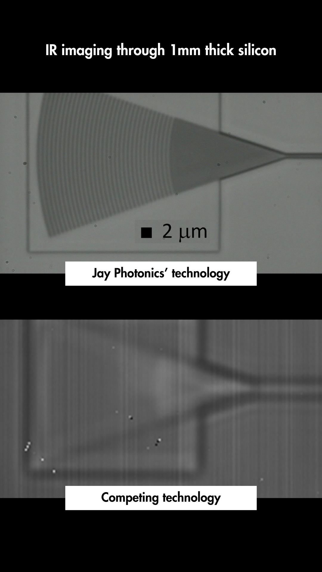
Addressing the needs of chip designers and R&D teams, our technology tackles the long-standing challenge of silicon's opacity in microchip inspection, delivering high definition imaging for each silicon layer, even in tightly stacked configurations. Here's a demo showcasing the impressive capabilities of our microscope, which offers a cost effective alternative to traditional infrared microscopes. Images acquired in real time within seconds, with no sample preparation and no image post-processing.
20x
-

Existing technology
-

Our technology


Image of an integrated silicon chip sandwiched between two 500um thick silicon wafers
40x
-

Existing technology
-

Our technology


Image of an integrated silicon chip sandwiched between two 500um thick silicon wafers
100x
-

Existing technology
-

Our technology


Image of an integrated silicon chip sandwiched between two 500um thick silicon wafers
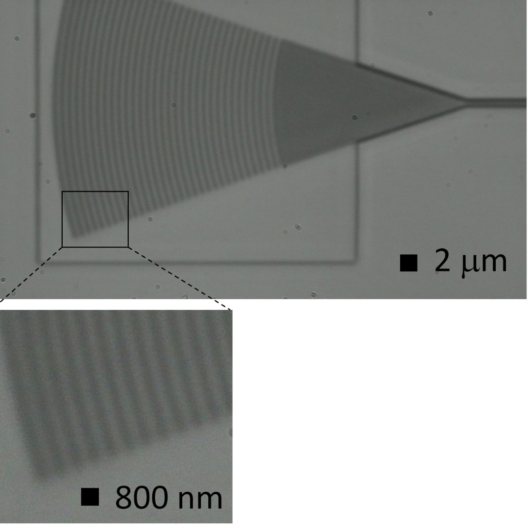
Even more precise
Our technology takes precision to the next level, delivering high-definition imaging of silicon layers with exceptional resolution.
Image of an integrated silicon chip sandwiched between two 500um thick silicon wafers
Our latest innovation : Si-Through-HR microscope
The Si-Through-HR Infrared Transmission Microscope
Groundbreaking solution for nondestructive inspection through silicon layers.
- Deep silicon imaging with superior resolution and high-definition clarity
- Affordable ready-to-use design
- Perfect for real-time inspection of silicon chips under microscopes and R&D applications
Upgrade your lab with accessible, cutting edge technology today.
Some of our clients


Microscope add-ons: Enhance your Jay Photonics microscope’s capabilities
-
SWIR polarizers kit for Jay Photonics Si-Through-HR microscope
Regular price $380.00 USDRegular priceUnit price per -
Darkfield condenser (Dry NA 0.7 - 0.9) for Jay Photonics Si-Through-HR microscope
Regular price $570.00 USDRegular priceUnit price per -
Darkfield kit for Jay Photonics Si-Through-HR microscope
Regular price $1,700.00 USDRegular priceUnit price per


What experts say about our technology
-

Philippe Lassonde, Research agent, National Institute of Scientific Research
"This microscope is ideal to observe silicon inside volume. The resolution and contrast of the images are impressive."
-

Steeve Morency, Expert Technician in Glass Materials, Center for Optics, Photonics and Lasers
"It's truly amazing to see such an affordable microscope delivering superior results compared to our $100,000 microscope!"
-

Mathieu Lebeuf, Test & Characterization Engineer, AEPONYX inc.
"Jay Photonics' microscope is a compact, user-friendly, competitively priced infrared inspection station with great potential."
-

Antoine Dumont, Field Application Scientist, Telops
"Very impressive technology!"
-

Philippe Labranche, Engineering Physics Technician, Laval University
"It's proof that technology can be 'simple' and exceptional at an incredible price!"


